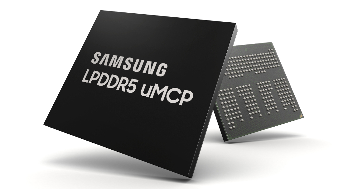
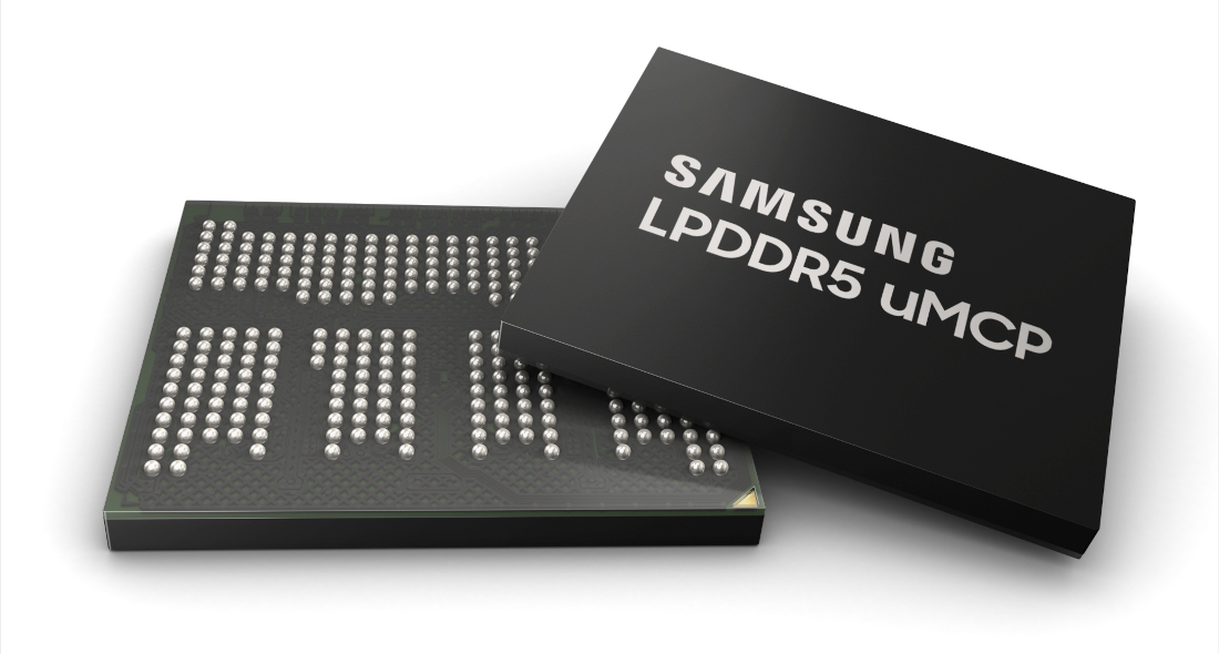
Samsung Electronics, one of the largest supplier of memory technology in the world, has begun mass production of their LPDDR5 UFS-based multichip package (uMCP) smartphone memory solution. These chips combine both LPDDR5 DRAM with the latest UFS 3.1 NAND flash, to provide improved memory performance for a wide-range of smartphones.
With both DRAM and NAND interfaces built-in, Samsung uMCP is great at providing fast speeds and high storage capacity at very low power. These advantages are crucial for various 5G applications such as advanced photography, graphics-intensive gaming and augmented reality.
The new chips are capable of DRAM performance levels of 25GB/s, NAND flash performance at 3GB/s, all within a package size that measures only 11.5mm x 13mm. Samsung will offer DRAM capacities ranging from 6 gigabytes (GB) to 12GB and storage options from 128GB to 512GB for these chips.
Samsung has already completed compatibility testing of the LPDDR5 uMCP and expects uMCP-equipped devices to hit mainstream markets starting this month.
Commenting on the launch, Young-soo Sohn, vice president of the Memory Product Planning Team at Samsung Electronics said:
Samsung’s new LPDDR5 uMCP is built upon our rich legacy of memory advancements and packaging know-how, enabling consumers to enjoy uninterrupted streaming, gaming and mixed reality experiences even in lower-tier devices. As 5G-compatible devices become more mainstream, we anticipate that our latest multichip package innovation will accelerate the market transition to 5G and beyond, and help to bring the metaverse into our everyday lives a lot faster.