
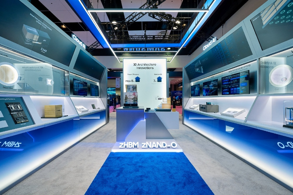
At the Future of Memory and Storage (FMS) 2026 conference in Santa Clara, California, Samsung Electronics presented its latest portfolio of artificial intelligence (AI) memory innovations and an updated technology roadmap.
Featuring an AI cloud server-inspired exhibition showcasing approximately 30 memory and storage technologies, the company outlined its strategic response to the increasing bandwidth and power demands of high-performance computing (HPC) and AI infrastructure.
3D Architectural Innovations: zHBM and zNAND-O
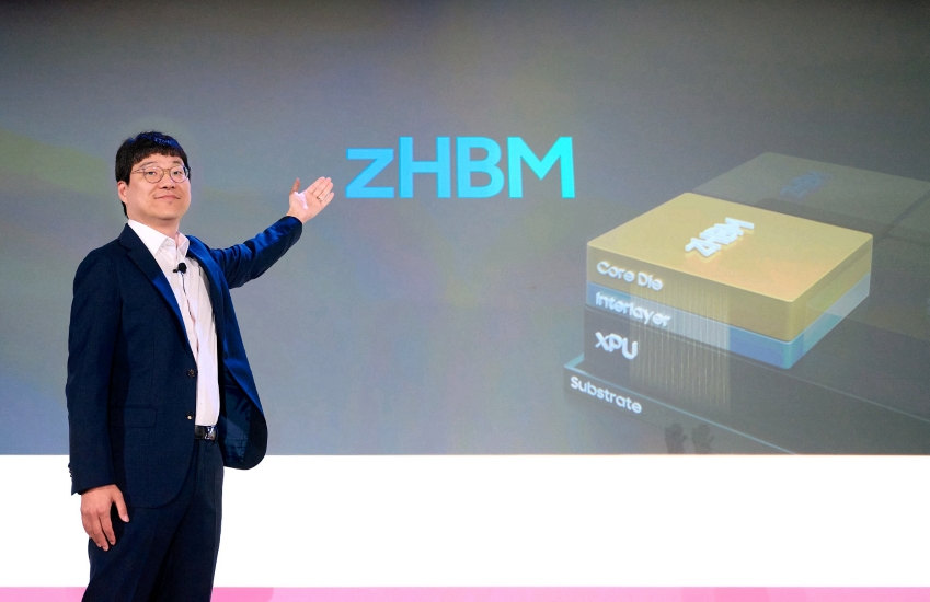
During the opening keynote titled “Driving the Wave of AI Revolution: 3D Innovations in Memory & Storage Architecture,” Samsung executives Jin-Yub Lee, Executive Vice President and Head of Flash Product & Technology, and Kyungryun Kim, Vice President and Project Leader of the DRAM Design Team, outlined the company’s vision for 3D memory structures.
Samsung introduced concept models for two new 3D architectures tailored for AI workloads:
- zHBM (Vertical Stacking): Moving away from conventional side-by-side placements, zHBM vertically stacks High Bandwidth Memory directly on top of AI accelerators. By using wafer bonding technology and reducing signal travel distance, the system aims to achieve up to eight times the performance and more than ten times the memory density of HBM5. The design also targets a threefold increase in energy efficiency and cuts thermal resistance by more than half. Additionally, zHBM supports custom interlayer intellectual property (IP) integration between the processor and memory.
- zNAND-O (Edge AI Storage): Built on Samsung’s V-NAND foundation, zNAND-O is in development in four- and eight-layer configurations. It focuses on high spatial efficiency, improved I/O speeds, and low latency to support real-time data processing in edge computing environments.
Introduction of V10 BV-NAND Architecture
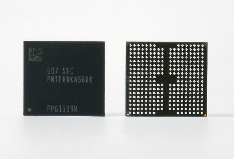
Marking 13 years since the debut of its initial V-NAND technology, Samsung unveiled V10 BV-NAND, the industry’s first memory based on a Bonding V-NAND architecture.
| Specification / Feature | V10 BV-NAND Details |
| Layer Count | 400+ vertical layers |
| Manufacturing Process | Wafer bonding technology for cell stacking |
| Density Improvement | ~58% increase over previous-generation V9 |
| Performance Gains | Improved read, write, and overall I/O speeds |
Comprehensive AI Memory and Enterprise Storage Roadmap
Samsung outlined updates across its broader product portfolio spanning DRAM, NAND, processing-in-memory (PIM), and enterprise drives:
- High Bandwidth Memory (HBM): Following the mass production of HBM4 using 1c DRAM and a 4-nanometer (nm) base die in February, Samsung initiated customer shipments of HBM4E samples in May. The company also presented concept previews for HBM5.
- Processing-In-Memory (PIM): Samsung showcased LPDDR5X-PIM, an mobile memory solution that executes data processing within the memory module itself to minimize data movement and decrease overall power consumption.
- Enterprise Solid-State Drives (SSDs): Updated storage models, including the PM1763 and BM1773, were highlighted to address capacity and throughput requirements in high-density AI data centers.
End-to-End Integrated Manufacturing Strategy
Positioning itself as an Integrated Device Manufacturer (IDM) with operations covering memory design, foundry fabrication, and advanced packaging, Samsung highlighted its ability to provide turnkey development. By consolidating design through mass production within a single pipeline, the company aims to reduce time-to-market and streamline power and performance optimization for customized AI hardware configurations.