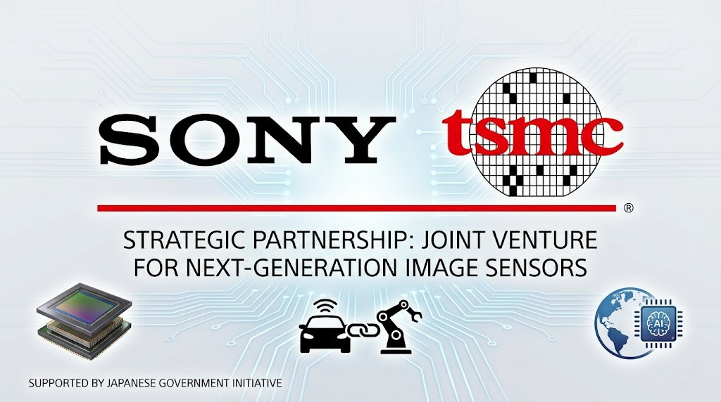
Sony Semiconductor Solutions Corporation and Taiwan Semiconductor Manufacturing Company Limited (TSMC) have signed a non-binding memorandum of understanding (MOU) outlining a new strategic partnership. The agreement details plans to collaborate on the development and manufacturing of next-generation image sensors.
Structure of the Proposed Joint Venture
Under the proposed terms, the two technology companies intend to establish a joint venture (JV), with Sony operating as the majority and controlling shareholder.
The JV’s development and production lines are slated to be housed within Sony’s newly constructed fabrication facility in Koshi City, Kumamoto Prefecture. The partnership is designed to integrate the core competencies of both firms, combining Sony’s background in image sensor design with TSMC’s established process technology and manufacturing infrastructure.
Investment and Expansion Strategy
Following the signing of the MOU, Sony and TSMC are currently in discussions regarding the financial framework of the joint venture. The proposed strategy includes:
- Phased Rollout: Investments by the JV will be implemented in stages, calibrated to align with shifting market demand.
- Government Support: The execution of these plans is operating on the premise of financial and logistical support from the Japanese government.
- Additional Domestic Investment: Concurrently, Sony is considering further capital investments to expand operations at its existing plant in Nagasaki.
Targeting Emerging Technologies
Beyond standard image sensor production, the collaboration is explicitly aimed at addressing the expanding market for physical artificial intelligence (AI) applications. The companies have identified the automotive and robotics sectors as primary areas of focus for future technological expansion and innovation.
Current Status
The current MOU is non-binding. The final establishment of the joint venture and the commencement of shared operations are contingent upon the execution of a definitive, legally binding agreement and the satisfaction of customary closing conditions.
Regarding this, Shinji Sashida, President and CEO of Sony Semiconductor Solutions Corporation, said:
Building on the trust cultivated through our long-standing collaboration with TSMC, I am delighted that we have reached an agreement to advance our partnership to a new stage. This JV is a significant initiative that brings together the strengths of both companies and aims to drive further advancement in technology and business within the next-generation image sensor field. Building on this JV, Sony intends to further strengthen its business operations with a focus on creating high added value. Rooted in the Sony Spirit that has guided us since our founding, we intend to continue to take on the challenge of creating new markets through unprecedented ideas and distinctive technologies.
TSMC Senior Vice President and Deputy Co-COO, Dr. Kevin Zhang, said:
Sony has been our long-time partner in the CMOS image sensor business. We are excited to elevate our collaboration to the next level, which represents a key step forward in driving future sensing technology in the AI era. This partnership underscores our shared commitment and mutual vision of leveraging cutting-edge technologies and innovative solutions to deliver leading sensing technology and products. We look forward to working closely together to achieve impactful results and create lasting value for all stakeholders.