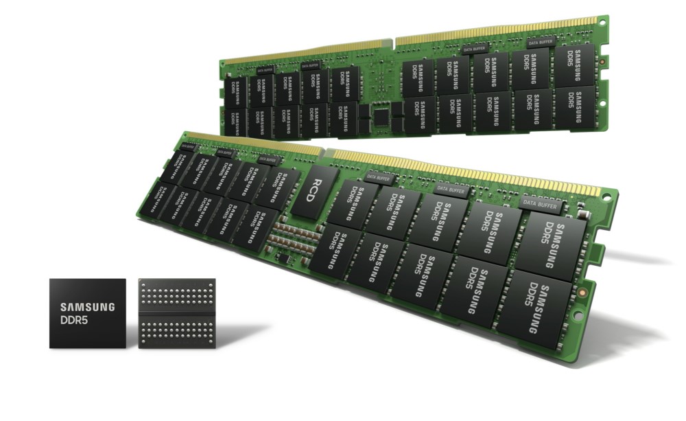
Samsung, which has been producing DRAMs for a long time now has today announced that it has begun the mass production of 14-nanometer DRAM based on extreme ultraviolet (EUV) technology. This comes after the company shipped 1 million EUV DRAM modules back in March 2020.
The latest DDR5 DRAM from Samsung now features multi-layer EUV which enables extreme miniaturization and that was something not possible with the conventional argon fluoride (ArF) process, says the company. With 5 EUV layers on the 14nm DDR5 DRAM, Samsung says that the overall wafer productivity has increased by 20% (approx.) and the power consumption has come down by nearly 20%.
As for the speeds, the 14nm DDR5 DRAM can achieve up to 7.2 Gbps and the company plans to expand its portfolio to support supercomputers, data center, and enterprise server applications.
Commenting on this, Jooyoung Lee, Senior Vice President and Head of DRAM Product & Technology at Samsung Electronics said:
We have led the DRAM market for nearly three decades by pioneering key patterning technology innovations. Today, Samsung is setting another technology milestone with multi-layer EUV that has enabled extreme miniaturization at 14nm — a feat not possible with the conventional argon fluoride (ArF) process. Building on this advancement, we will continue to provide the most differentiated memory solutions by fully addressing the need for greater performance and capacity in the data-driven world of 5G, AI, and the metaverse.