Samsung back in September last year announced that it is working on 7LPP (Low Power Plus) with EUV (extreme ultra violet) lithography technology for smartphones that is targeted for initial production in the second half of 2018. Earlier this Feburary it announced that it is building new EUV (extreme ultraviolet) line in Hwaseong, Korea. Earlier this week the company started wafer production of its revolutionary process node, 7LPP, the 7-nanometer (nm) LPP (Low Power Plus) with extreme ultraviolet (EUV) lithography technology.
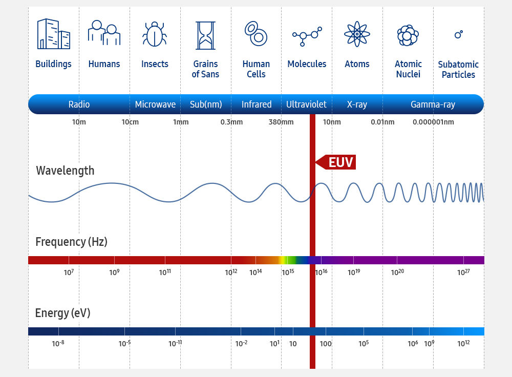
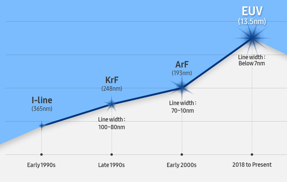
The EUV system, which utilizes extreme ultraviolet technology, can perform photolithography process by using a light source with EUV wavelength. In the world of chip manufacturing, realizing finer circuits is vital as it enables integration of more components inside a chip, which helps build those with higher power and energy efficiency. Upcoming EUV scanners will utilize EUV radiation at a 13.5nm wavelength, less than 1/14 of what current ArF excimer laser scanners are able to provide.
EUV uses 13.5nm wavelength light to expose silicon wafers as opposed to conventional argon fluoride (ArF) immersion technologies that are only able to achieve 193nm wavelengths and require expensive multi-patterning mask sets. EUV enables the use of a single mask to create a silicon wafer layer where ArF can require up to 4 masks to create that same layer. Consequently Samsung’s 7LPP process can reduce the total number of masks by about 20% compared to non-EUV process, enabling customers to save time and cost.
The EUV lithography improvements also deliver increased performance, lower power and smaller area while improving design productivity by reducing mulit-patterning complexity.
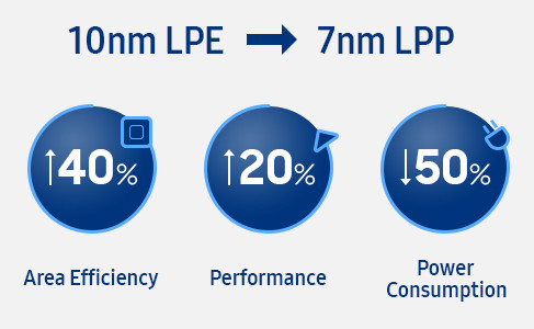
Compared to its 10nm FinFET predecessors, Samsung’s 7LPP technology not only greatly reduces the process complexity with fewer layers and better yields, but also delivers up to a 40% increase in area efficiency with 20% higher performance or up to 50% lower power consumption.
Earlier this year Samsung and Qualcomm announcedthat they have expanded their foundry partnership for on EUV process technology and also said that future Snapdragon 5G mobile chipsets will use Samsung’s 7nm LPP EUV process technology.
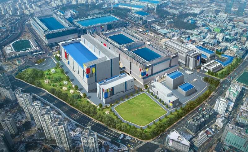
By 2020, Samsung expects to secure additional capacity with a new EUV line for customers who need high-volume manufacturing for next-generation chip designs. It already said that initial investment in the new EUV line is expected reach US$ 6 billion by 2020.
Samsung has also developed proprietary capabilities such as a unique mask inspection tool that performs early defect detection in EUV masks, allowing those defects to be eliminated early in the manufacturing cycle.