
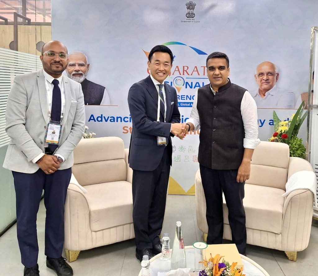
FUJIFILM India has signed a Memorandum of Understanding (MoU) with the Gujarat State Electronics Mission (GSEM), Department of Science and Technology (DST), Government of Gujarat. Announced at the Vibrant Gujarat Regional Conference in Vadodara, the agreement establishes a framework for the company to explore manufacturing opportunities for semiconductor materials in India and develop domestic supply chain capabilities.
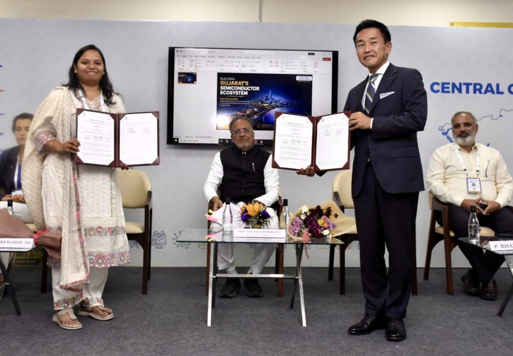
The collaboration comes as India actively pursues its objective of establishing itself as a global hub for semiconductor manufacturing. Through this partnership, FUJIFILM India intends to assess the feasibility of setting up a semiconductor materials production base in the Dholera Special Investment Region (SIR).
The company plans to engage with government stakeholders, industry organizations, and private enterprises to support the development of the localized supply chain.
Strategic Framework and Market Demand
The initiative aligns with broader national manufacturing strategies, specifically the Government of India’s “Make in India” initiative, which emphasizes localized production, technology collaboration, and supply chain infrastructure.
The domestic and global demand for semiconductors is experiencing sustained growth across multiple critical sectors:
- Consumer Electronics: Smartphones, computing hardware, and smart devices.
- Automotive: Advanced driver-assistance systems (ADAS) and electric vehicle (EV) components.
- Telecommunications: 5G infrastructure and next-generation networking equipment.
- Artificial Intelligence: High-performance computing systems and data centers.
By exploring localized production of critical raw materials, the initiative aims to reduce import dependencies and enhance India’s self-reliance and positioning within the global semiconductor value chain.
Global Infrastructure and Outlook
Fujifilm Electronic Materials currently operates more than 20 production bases worldwide, supplying advanced chemical and material solutions essential to the semiconductor fabrication process. The company has identified India as a strategic market for long-term growth and innovation within its global portfolio.
The execution of this MoU represents an initial step toward developing a sustainable, localized manufacturing infrastructure intended to support the country’s long-term semiconductor production targets.
Commenting on the occasion, Koji Wada, Managing Director, FUJIFILM India, said:
At FUJIFILM India, we have been closely assessing opportunities across the Indian market and evaluating how our diverse businesses can contribute to the country’s long-term growth and innovation ambitions. This MoU marks an important milestone in that journey and brings us a step closer to realizing our plans for investment in Dholera. Guided by our Group Purpose of ‘Giving our world more smiles,’ we believe innovation should create meaningful value for society. By supporting the development of critical technologies and manufacturing capabilities in India, we hope to contribute to economic growth and technological advancement of the nation.
Abhi Shekhar Singh, National Head – Strategy & Business Development, Electronic Materials Division, FUJIFILM India added:
FUJIFILM Electronic Materials develops and manages chemical formulations that power the most critical processes of semiconductor technology. We are a diverse, global supplier that delivers tailored support where our customers need us most. The spirit of partnership drives everything we do, our commitment to the continued success and innovation of our customers is our primary focus. Globally, Fujifilm recognizes its vital role in supporting and advancing many of the changes we see in our everyday lives and now we are gearing up to introduce our technology to the semiconductor ecosystem in India which will support Today’s aspirational India which will guarantee of tomorrow’s Viksit Bharat.