Cadence Design Systems and the Indian Institute of Technology Delhi (IIT Delhi) have announced the establishment of the IIT Delhi–Cadence Innovation Lab.
Operating as a multidisciplinary centre of excellence, the facility is designed to provide students, researchers, and early-stage startups with access to industry-grade electronic design automation (EDA) software and artificial intelligence (AI)-enabled workflows.
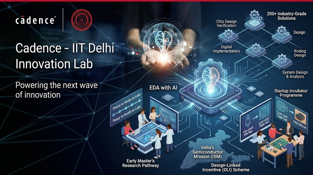
The initiative aligns with the strategic objectives of the India Semiconductor Mission (ISM) and the government’s Design-Linked Incentive (DLI) scheme, both of which aim to expand domestic semiconductor design capabilities and strengthen the engineering workforce.
Industry-Standard Tools and AI Integration
The new lab provides access to more than 200 Cadence solutions, spanning four primary engineering domains:
- Chip design verification
- Digital implementation
- Analog design
- System design and analysis
By incorporating AI-driven methodologies into these traditional workflows, the lab aims to train users in modern very large-scale integration (VLSI) design techniques, focusing on optimizing engineering productivity and system performance through automation.
Curriculum Update and Practical Training
To transition away from purely theoretical instruction, IIT Delhi has integrated Cadence-developed courseware into its academic curriculum. The updated modules pair fundamental engineering theory with project-based lab assessments and real-world problem statements.
To bridge academic learning with commercial technology roadmaps, the curriculum will be supplemented by guest lectures from Cadence engineers and semiconductor industry practitioners.
Research Pathways and Startup Incubation
The lab is introducing an Early Master’s Research pathway targeted at select fourth-year undergraduate students from Indian Institutes of Technology (IITs) and National Institutes of Technology (NITs). Participating students will receive joint mentorship from IIT Delhi faculty and Cadence technical experts across various research disciplines.
Additionally, the facility includes an incubator programme designed to assist pre-seed startups. Evaluated on a case-by-case basis, selected startups will receive low-cost access to development tools to help navigate the path to first tape-out (the final design stage before manufacturing) and the creation of working physical prototypes.
The long-term objectives of the collaboration include increasing academic research output, improving graduate readiness for immediate industry deployment, and establishing a structured pipeline to translate academic design concepts into commercial industrial outcomes.
Alok Jain, Corporate VP and India Managing Director, Cadence, said:
Students at IIT Delhi now use the same AI‑enabled tools they’ll see on day one in industry, closing the gap from classroom to tapeout. Pairing industry‑grade technology with project‑based curricula, real‑world challenges, and targeted startup support strengthens research relevance and workforce readiness for India’s semiconductor future.
Prof. Jayadeva, Prof. In-Charge, Cadence-IIT Delhi Innovation Lab, said:
The IIT Delhi–Cadence Innovation Lab combines top-tier academic rigor with cutting-edge industry tools. This partnership will expand research output, prepare students for high-impact careers, and help founders move from ideas to prototypes, supporting the goals of the India Semiconductor Mission and the DLI scheme.