Samsung announced back in April that its second generation 10-nanometer (nm) FinFET process technology, 10LPP (Low Power Plus), has been qualified and is ready for production. Today the Korean giant has announced that its Foundry Business has started mass production of these SoCs based on second-gen 10nm process tech, 10LPP .
This will be used in the Exynos 9 Series 9810 SoC that has3rd generation custom designed CPU cores and has LTE Cat.18 6CA-supported modem with maximum download speed of up to 1.2Gbp (Cat.18).
The 10LPP will feature enhanced 3D FinFET structure that promises up to 10% higher performance along with 15% lower power consumption compared to the first generation 10LPE (Low-Power Early) process with the same area scaling.
“As this process is derived from the already proven 10LPE technology, it offers competitive advantages by greatly reducing turn-around time from development to mass production and by providing significantly higher initial manufacturing yield,” said Samsung.
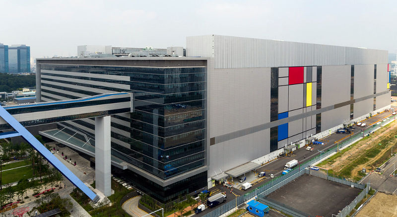
The company already announced newest S3-line in Hwaseong, Korea, third fab of Samsung’s Foundry Business, following S1 in Giheung, Korea and S2 in Austin, USA to meet long-term demand for the 10nm process. Samsung has confirmed that 7nm FinFET process technology with EUV (Extreme Ultra Violet) will also be mass produced at S3.
Samsung said that SoCs designed with 10LPP process technology will available early next year and are expected to become more widely available throughout the year. So we can expect it in the upcoming flagship Galaxy S9 series in early 2018.