

Tata Electronics and FUJIFILM Corporation have entered into a Memorandum of Understanding (MoU) to establish and accelerate a localized semiconductor materials supply chain in India.
The collaboration focuses on developing and supplying specialized materials tailored to Tata Electronics’ upcoming commercial semiconductor fabrication facility in Dholera, Gujarat.
The agreement aligns with broader national efforts to expand India’s presence within the global semiconductor manufacturing value chain by establishing domestic supply networks for critical fabrication inputs.
Localized Supply Chains and Technical Collaboration
A central focus of the partnership is strengthening supply chain resilience by localizing the production of essential raw materials required for chip manufacturing. Under the MoU, Fujifilm will provide technical support to domestic chemical suppliers, sharing expertise in quality assurance and manufacturing processes to facilitate the production of high-purity chemicals within India.
Key Facility and Investment Details
| Parameter | Tata Electronics Fab | Fujifilm Materials Plant |
| Location | Dholera Special Investment Region (DSIR), Gujarat | Dholera Special Investment Region (DSIR), Gujarat |
| Estimated Investment | ₹91,000 crore (~US$11 billion) | ~₹800 crore (~US$83 million) |
| Operational Scope | 300 mm (12-inch) wafer manufacturing; 28 nm to 110 nm process nodes | Phased production of advanced semiconductor materials |
| Target Sectors | Automotive, consumer electronics, AI, data storage, wireless communications | Direct supply to fabrication facilities |
Strategic Implications for Dholera Fab
Fujifilm’s phased investment in DSIR positions the company as an early participant in the localized materials ecosystem serving the Dholera facility. Tata Electronics’ 300 mm wafer fab is designed to address mature and legacy process nodes ranging from 28 nm to 110 nm, which serve core sectors such as automotive systems, consumer devices, data storage, and artificial intelligence hardware.
By integrating materials manufacturing adjacent to the fabrication site, the collaboration aims to mitigate logistics risks and secure direct access to the chemical and material inputs required for ongoing fab operations.
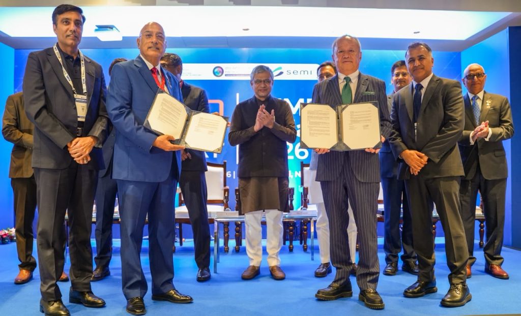
Dr. Randhir Thakur, CEO & MD, Tata Electronics, said:
Tata Electronics is committed to building a resilient, world-class semiconductor manufacturing ecosystem in India. Our strategic partnership with Fujifilm marks an important step in strengthening the semiconductor materials supply chain for our Dholera Fab. By combining Fujifilm’s expertise in advanced semiconductor materials with Tata Electronics’ vision of creating a robust manufacturing base, we are enhancing supply chain resilience for our global customers, accelerating ecosystem development, and supporting India’s ambition to become a trusted global hub for semiconductor manufacturing. This will go a long way in building the foundation for a secure semiconductor value chain serving customers in India and around the world.
Teiichi Goto, President, Representative Director & Chief Executive Officer, FUJIFILM Holdings Corporation, Japan, said:
Fujifilm positions its semiconductor materials business as a key growth driver for Fujifilm Group and recognizes India’s rapidly expanding semiconductor market as a critical opportunity for further business expansion. We are confident that the partnership between Tata Electronics, a leader in shaping the semiconductor ecosystem in India, and Fujifilm, with its comprehensive range of semiconductor materials spanning the semiconductor manufacturing process from front-end to back-end, will play a pivotal role in advancing the country’s semiconductor industry.
Tetsuya Iwasaki, Director, Executive Vice President and General Manager, Electronic Materials Business Division, FUJIFILM Corporation, added:
We are honored to support India’s vision of strengthening its advanced manufacturing and technology capabilities through this partnership. Fujifilm offers a wide range of materials used throughout the entire semiconductor manufacturing process, from front-end to back-end. These materials include photoresists, photolithography-related materials, CMP slurries, post-CMP cleaners, thin-film materials, photosensitive insulating materials such as polyimides under the ZEMATES™ brand, and high-purity process chemicals. Fujifilm also provides Wave Control Mosaic™, a group of functional materials including color filter materials for image sensors. I am sure this partnership will help us develop a good semiconductor materials ecosystem in India.