
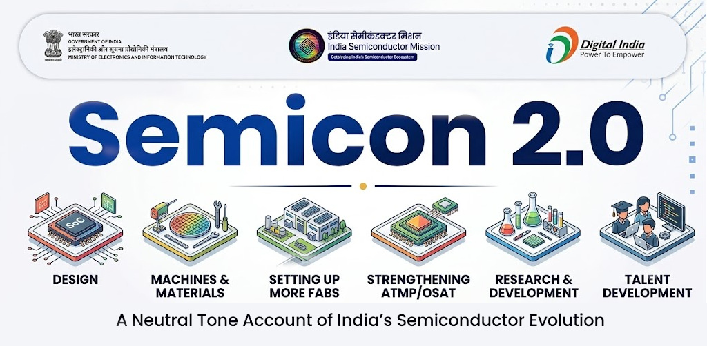
The Government of India has officially notified the six pillars governing the Semicon 2.0 Scheme, marking a major policy expansion aimed at developing a comprehensive domestic semiconductor design and manufacturing ecosystem.
The notification outlines fiscal incentives, eligibility parameters, and implementation guidelines across the entire semiconductor value chain.
Objectives and Strategic Scope
Building on the foundation laid under the initial Semicon India Programme, Semicon 2.0 aims to enhance supply chain resilience, reduce external dependencies, support long-term economic growth, and bolster national security. The program covers 10 categories divided across six key pillars:
Pillar 1 – Design:
- Category 1 (Strategic Priorities): Supports the design of semiconductor IPs, Chips, SoCs, and Modules tailored for national importance and critical infrastructure. IP rights under this category are co-owned with the Centre for Development of Advanced Computing (C-DAC).
- Category 2 (Commercial Sector): Extends design infrastructure support, seed funding (up to ₹15 crore), equity co-investment, and royalty financing for domestic fabless companies, startups, and MSMEs.
- Category 3 (Deployment-Linked Incentive – DLI): Provides an incentive of 9% on net sales for up to five years for newly launched products, capped at ₹30 crore per application and ₹120 crore per company.
Pillar 2 – Machines and Materials (Category 4):
- Covers raw materials (wafers, photoresists, chemicals, specialty gases), equipment R&D, refurbished/capital machinery, and testing facilities.
- Offers 30% capital expenditure support on a pari-passu basis, alongside a 5-year graded Production Linked Incentive (PLI) of 2%–10% on domestic Bill of Materials (BoM) for equipment manufacturers starting FY 2028–29.
Pillar 3 – Semiconductor & Display Fabs:
- Category 5 (Silicon Wafer Fabs): 40% fiscal support on a pari-passu basis for 300 mm wafer fabs with a minimum capacity of 40,000 wafer starts/month and a minimum capital investment threshold of ₹20,000 crore
- Category 6 (Compound, Photonics, Sensors/MEMS, Discrete Fabs): 35% fiscal support on a pari-passu basis with an investment threshold of ₹500 crore.
- Category 7 (Display Fabs): 35% fiscal support on a pari-passu basis for OLED, Micro LED, and Gen-8+ LCD fabs.
Pillar 4 – Packaging Facilities (Category 8):
- Offers 35% fiscal support on pari-passu capital expenditure for Advanced Packaging (2.5D/3D packaging, wafer-level packaging, heterogeneous integration) and 25% fiscal support for legacy packaging facilities.
Pillar 5 – Research and Development (Category 9):
- Provides fiscal assistance of up to 75% of combined capex and opex project costs (inclusive of state incentives) for research in advanced process nodes, silicon photonics, and chiplet technologies.
Pillar 6 – Talent Development (Category 10):
-
-
Provides up to 75% project cost support to academic institutions, research laboratories, and domestic training centers to expand training across design, fabrication, and shop-floor operations.
-
Implementation and Governance
The India Semiconductor Mission (ISM) serves as the nodal agency responsible for appraisal, recommendation, and operational oversight under the scheme. Key operational frameworks include:
- Approval Tiers: Design and talent development proposals under ₹100 crore will be approved by the Secretary, MeitY; projects between ₹100 crore and ₹500 crore by the Minister for Electronics and IT; and projects exceeding ₹500 crore—along with all manufacturing/fab categories—by the Union Cabinet.
- Application Window and Duration: The application window is initially slated for three years, with supported project durations running up to six years. A mid-term impact assessment will be conducted after three years of implementation.
- Deep-Tech Recognition: ISM may also introduce dedicated Semiconductor Deep Tech Awards starting in 2026 to encourage niche research and development.
Industry Progress and Projections
During the briefing, Union Minister Ashwini Vaishnaw highlighted key benchmarks achieved under the initial phase of the semiconductor initiative:
- Talent Scale: India surpassed its original target of preparing 85,000 semiconductor engineers over a 10-year horizon within four years, setting a subsequent target to train an additional 100,000 engineers.
- Speed of Execution: Approvals for several operational projects were processed in cycles ranging from 90 to 200 days, with commercial production commencing at select facilities within 13 months of groundbreaking.
- Employment and Market Share: Domestic initiatives are projected to generate approximately 50,000 to 60,000 direct jobs, with the Indian market anticipated to account for roughly 10% of global semiconductor demand in the coming years.