
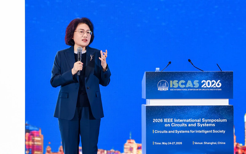
Today, at the 2026 IEEE International Symposium on Circuits and Systems (ISCAS), HUAWEI presented its new Tau (τ) Scaling Law, a new principle for guiding the future development of the semiconductor industry. Historically, the semiconductor industry has relied on Moore’s law to reduce chip size and increase the number of transistors.
This law, according to HUAWEI, proposes replacing geometric scaling (Moore’s law logic) with time (τ) scaling as a new guiding principle for the evolution of both semiconductors and electronic systems.
Moore’s Law in Mobile Processors
Moore’s Law states that the number of transistors on a microchip roughly doubles every two years, improving computing performance while reducing costs. Chipmakers achieve this by shrinking transistor sizes, allowing chips to become faster, more power-efficient, and cooler.
Mobile processor manufacturers and foundries such as TSMC and Samsung rely on this process to deliver higher performance with efficient power consumption. Currently, the Mobile processor industry is in 3nm process technology and moving towards 2nm.
Shrinking silicon beyond 3nm requires ultra-complex machinery such as High-NA EUV lithography, which contradicts Moore’s law of reduced cost per generation.
HUAWEI’s Tau (τ) Scaling Law
And HUAWEI exactly addresses this issue with its new Tau (τ) Scaling Law. By replacing geometric scaling with time (τ) scaling, innovative technologies such as LogicFolding can be used to continuously compress signal propagation delay and steadily improve transistor density, which will drive the ongoing evolution of semiconductors and electronic systems.
This tech would reduce signal delay across devices, circuits, chips, and full systems, eventually increasing performance.
LogicFolding Architecture
Based on this law, HUAWEI has developed innovative core technologies like LogicFolding and established a multi-level co-optimization mechanism that spans semiconductor devices, circuits, chips, and systems.
This mechanism aims to systematically shorten the time constant τ in order to drive up performance, energy efficiency, and transistor density at each level in the following ways:
- Device level: Reducing transistor and interconnect delay for better efficiency
- Circuit level: Shortening wiring paths to improve performance and density
- Chip level: Optimizing software and silicon together to reduce execution time
- System level: Using UnifiedBus to lower communication latency across systems
HUAWEI Kirin Chips based on Tau (τ) Scaling Law
HUAWEI claims to have already designed and mass-produced 381 chips based on the τ Scaling Law. At her keynote speech, elaborating on the application of the τ Scaling Law to smartphones and AI computing, He Tingbo, from HUAWEI, announced that upcoming Kirin chips will follow this law and its new LogicFolding architecture.
The Kirin chips scheduled to launch in Fall 2026 will be the first ever to adopt the LogicFolding architecture, which will considerably enhance the chips’ performance, says the company.

Compared to a conventional System on Chip (SoC) design, LogicFolding design on 2026 Kirin Chips is said to bring 53.5% increase in transistor density, reaching up to 238 MTr/mm², 40% increase of P-core power efficiency, and a max clock frequency increase of 12.7%, reaching up to 3.1GHz by 2026.
By 2031, the high-end chips based on this LogicFolding architecture will feature a transistor density that is equivalent to 14 Å (1.4 nm) processes.
At the conference presentation, Ms. He Tingbo, President of the Semiconductor Business Dept, said,
We believe that openness and collaboration are key to driving ongoing progress in the semiconductor industry. No single company can independently find all the answers along the path of semiconductor evolution. With the τ Scaling Law, we look forward to working closely with scientists, engineers, and industry partners around the world to drive the sustainable development of the semiconductor and electronics industries.