During their 5th annual Foundry Forum (SFF) 2021, Samsung introduced their roadmap for their 3nm and 2nm process nodes based on the Gate-All-Around (GAA) transistor structure. According to the company, 3nm-based chip designs is scheduled to start production in the first half of 2022, while 2nm-based chips will arrive in 2025.
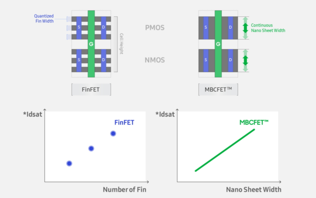
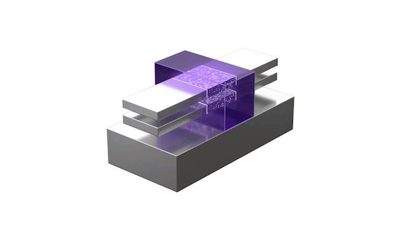
Samsung is continuously working towards migrating their process nodes to latest in the industry. The 3nm process node will utilize both GAA technology and Multi-Bridge-Channel FET (MBCFET) technology, resulting in up to 35 percent decrease in area, 30 percent higher performance or 50 percent lower power consumption when compared to the 5nm process node.
Samsung Foundry will begin production of their 3nm-based chip designs for customers in 2022, and the company also expects the 2nd generation of 3nm process to become available in 2023.
In regard to 2nm, Samsung is reportedly in the early stages of the process node’s development with MBCFET, and expects mass production to begin in 2025. Realistically, that means that the end consumer will see these chips in devices from 2026 onwards.