After reports, TSMC today announced that its 3 nm technology has successfully entered mass production with good yields. This was announced at a topping ceremony at its Fab 18 new construction site in the Southern Taiwan Science Park (STSP) today.
TSMC expects that 3nm technology will create end products with a market value of US$1.5 trillion within five years of production. It already announced that it is building 3nm capacity at its Arizona site, and Apple said that it will use its 3nm chips.
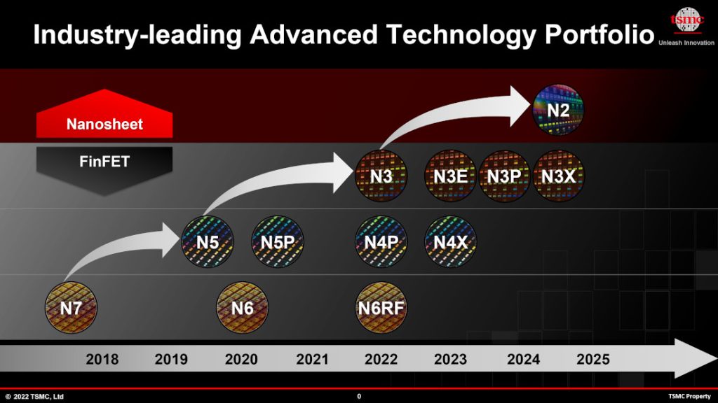
Compared to the 5nm (N5) process, TSMC’s 3nm process will offer up to 1.6X logic density gain and 30-35% power reduction at the same speed, and supports the innovative TSMC FinFLEX architecture.
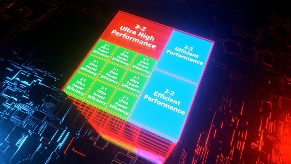
The FINFLEX architectural innovation offers choices of different standard cells with a 3-2 fin configuration for ultra performance, a 2-1 fin configuration for best power efficiency and transistor density, and a 2-2 fin configuration providing a balance between the two for Efficient Performance.
TSMC Fab 18, investments and 2nm fabs
Phases 1 through 8 of TSMC Fab 18 each have a clean room area of 58,000 square meters, approximately double the size of a standard logic fab.
The company said that its total investment in Fab 18 will exceed NT$1.86 trillion, creating more than 23,500 construction jobs and over 11,300 high-tech direct job opportunities.
TSMC said that it will open a global R&D Center in the Hsinchu Science Park in the second quarter of 2023. The company will is also be making preparations for its 2nm fabs, which will be located in the Hsinchu and Central Taiwan Science Parks, with a total of six phases proceeding as planned.