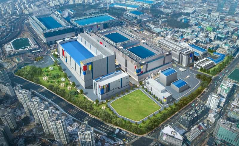
Samsung back in September announced that it is working on 7LPP (Low Power Plus) with EUV (extreme ultra violet) lithography technology for smartphones that is targeted for initial production in the second half of 2018. Today, as expected, the company has announced that it is building new EUV (extreme ultraviolet) line in Hwaseong, Korea.
Samsung will use EUV technology starting with its 7-nanometer (nm) LPP (Low Power Plus) process. Yesterday Samsung and Qualcomm announced that they have expanded their foundry partnership for on EUV process technology and also said that future Snapdragon 5G mobile chipsets will use Samsung’s 7nm LPP EUV process technology.
Samsung said that the new EUV line will enable to strengthen its leadership in single nanometer process technology to meet demand from various applications, including mobile, server, network, and HPC (high performance computing).
The new facility is expected to be completed within the second half of 2019 and will be ready for production in 2020. The initial investment in the new EUV line is expected reach USD 6 billion by 2020 and the company said that additional investment will be determined depending on market circumstances.